


The GPU Monopoly is Over. The New AI Infrastructure Stack Part 1 [Investigations]
A Hardware Investment Thesis for the Post-NVIDIA Era of ASICs, CXL, and Photonics

It takes time to create work that’s clear, independent, and genuinely useful. If you’ve found value in this newsletter, consider becoming a paid subscriber. It helps me dive deeper into research, reach more people, stay free from ads/hidden agendas, and supports my crippling chocolate milk addiction. We run on a “pay what you can” model—so if you believe in the mission, there’s likely a plan that fits (over here).
Every subscription helps me stay independent, avoid clickbait, and focus on depth over noise, and I deeply appreciate everyone who chooses to support our cult.
PS – Supporting this work doesn’t have to come out of your pocket. If you read this as part of your professional development, you can use this email template to request reimbursement for your subscription.
Every month, the Chocolate Milk Cult reaches over a million Builders, Investors, Policy Makers, Leaders, and more. If you’d like to meet other members of our community, please fill out this contact form here (I will never sell your data nor will I make intros w/o your explicit permission)- https://forms.gle/Pi1pGLuS1FmzXoLr6
Everyone’s talking about the rise of SLMs — Smaller, Specialized Language Models — because they’re more controllable, auditable, efficient. But the conversation always stops at the model layer.
As a great artist, it is my role to look beyond the interns and analyze what happens next. What has to change beneath and around the model to make this shift viable at scale? The answer is much more interesting than you’d think.
If you’ve followed our recent work, you already know the answer. The current AI stack is approaching a hard ceiling. Power budgets are maxed. Memory sits stranded. Inference costs are spiraling. General-purpose compute isn’t adapting — it’s cracking.

Think I’m exaggerating? Here’s what the numbers say:
NVIDIA's “B200 Tensor Core GPU can consume up to 1000 W or more under full load, making it one of the most power-hungry processors ever built”.
Large large portions of enterprise computing resources get stranded in their data centers (sometimes over 80%, although the range varies).
Diffusion inference TCO on cloud? $24M over 3 years. On-prem with optimized silicon? Under $8M.
Hyperscalers moving off merchant silicon are seeing $10B+ in projected savings.
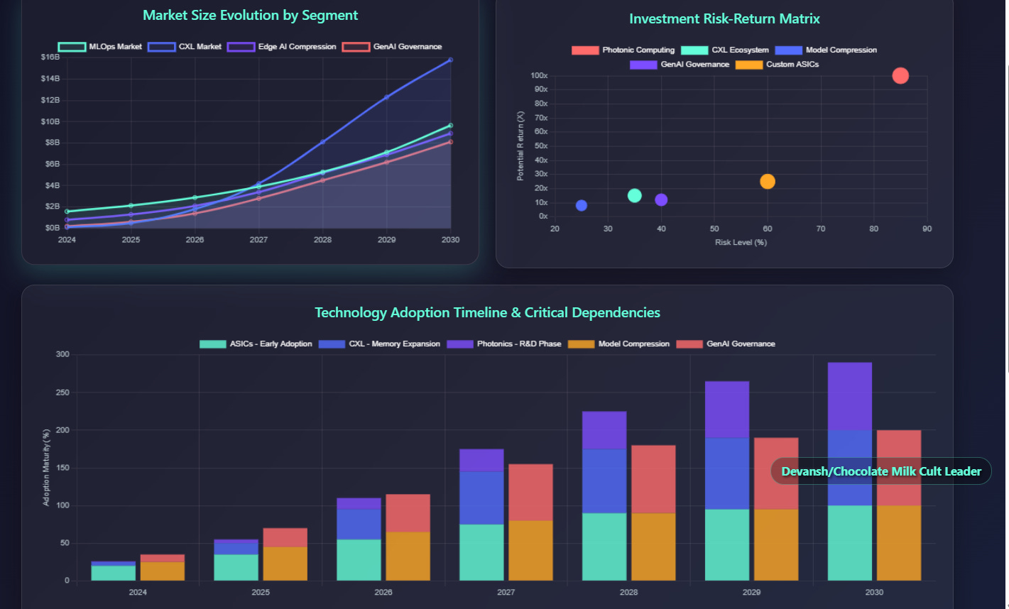
The CXL memory market will hit $15.8B by 2028.
GenAI governance is tracking toward $10B by 2030, driven by legal mandates — not speculation.
Viewed from the lens of my investing framework, an antithesis is forming, one that diverges from the general-purpose computing thesis towards a more specialized, decentralized, governance-friendly road.
In more concrete terms, there is a lot of space in rebuilding the infrastructure stack from the ground up to focus on opportunities like specialized chips, composable memory, optical interconnects, model compression, and governance built into the substrate.

This article is the first in a two-part series. Today we will focus on the physical limitations of these system breaks down. The old playbook — scale more, spend more, and build racks of Data Centers for simple mat-mul at scale — won’t survive the decade. We will follow this up with another piece looking at the talent, software, and governance angles into computing — all of which will have to change drastically to account for the upcoming hardware re-alignment that we will discuss today.
Cuda will no longer hard carry you, just the way my glorious king, Charles Olivera can no longer carry my ability to enjoy all that was beautiful in the world. We must retire them both, and brave the unknown to find new guiding lights for our existence (please forgive any minor mistakes; my eyes are still overflowing after Ilia slept my king)…

The journey will be difficult, but I know we can do it together. We will follow the age old wisdom — when fighting a giant, beat them down; one body shot at a time.
Let’s break it down.

Executive Highlights (TL;DR of the Article)
The general-purpose GPU era is breaking under its own weight. In its place, a new AI infrastructure regime is forming — defined by three co-evolving, interdependent shifts in hardware design:
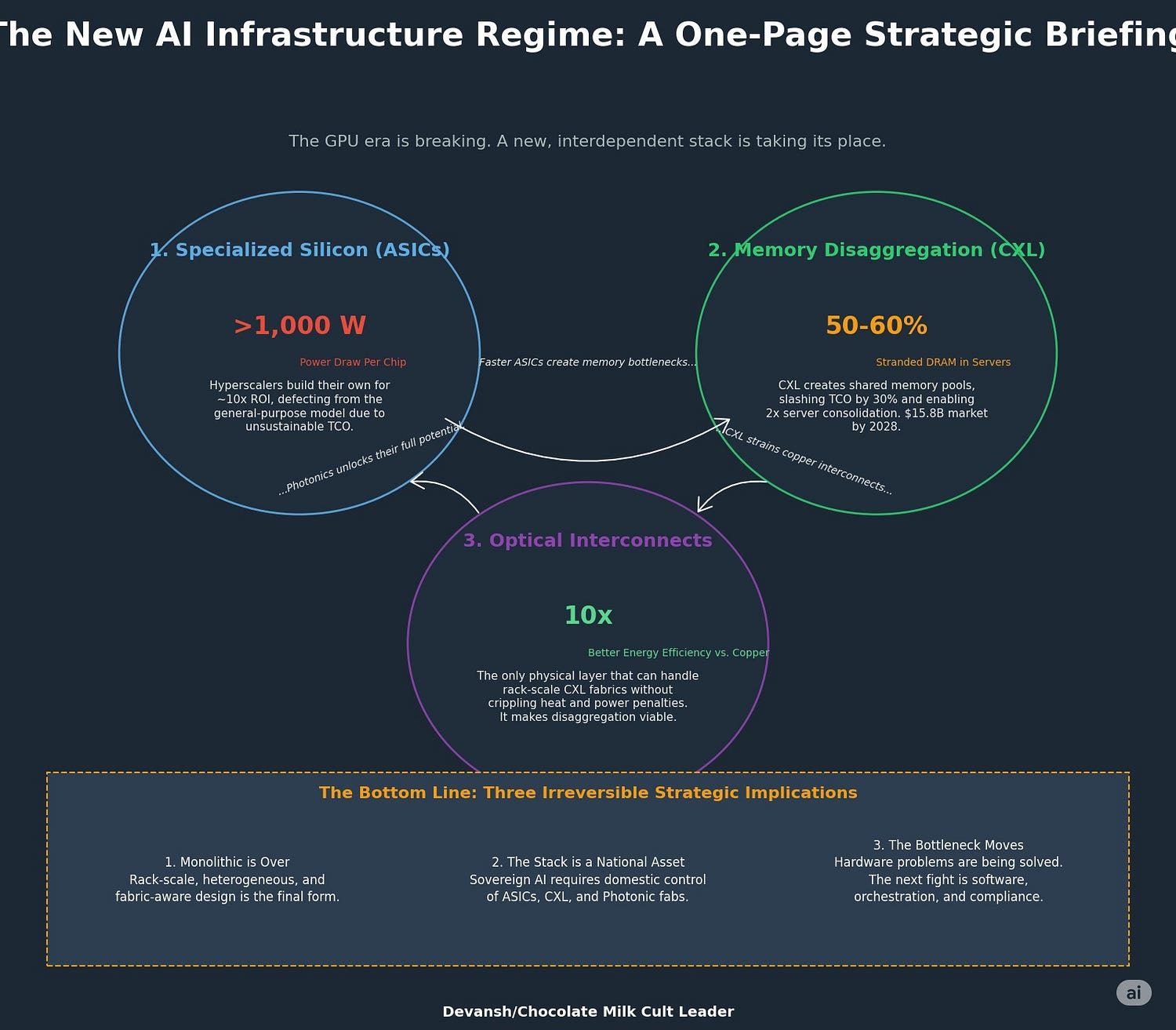
1. Specialized Silicon (ASICs)
NVIDIA’s B200 is the current peak — but also the ceiling. Power draw exceeds 1,000W per chip, forcing liquid cooling and creating structural TCO drag.
Hyperscalers are defecting. Google’s TPUs and AWS’s Trainium2 offer 2–5x efficiency gains and tighter stack integration.
Owning the chip stack offers hyperscalers a 10x ROI over five years. Renting from NVIDIA is no longer viable at scale.
2. Memory Disaggregation (CXL)
Most enterprise DRAM is stranded — locked to CPUs with 50–60% utilization.
CXL breaks this model by enabling pooled, shared memory across CPUs and accelerators.
Results: 25–30% TCO reduction in memory-heavy workloads, 2x server consolidation, and radically more efficient resource allocation.
The market for CXL-enabled memory and fabrics is projected to reach $15.8B by 2028.
3. Optical Interconnects (Photonics)
Copper interconnects cannot support the bandwidth and thermal limits of rack-scale memory fabrics.
Optical I/O (Ayar Labs, Celestial AI) enables multi-terabit connections with 10x better energy efficiency.
Photonic compute (Lightmatter, Q.ANT) is a longer-term play — replacing silicon math entirely with light for 10x energy and speed improvements.
Without optical I/O, pooled memory and disaggregated architectures stall at the physical layer.
Why These Three Are Not Modular — but Chained
Faster ASICs → create memory bottlenecks
CXL → fixes memory, but strains copper interconnects
Photonics → the only viable fabric to scale memory and compute across racks
Ignore one, and the others can’t scale. This isn’t a menu — it’s a dependency chain. And the adoption window is closing fast.
Strategic Implications
Monolithic server design is over. Rack-scale, heterogeneous, fabric-aware architectures are the future.
Sovereign AI strategy requires control over ASIC design, CXL protocols, and photonic packaging.
Hardware is no longer the bottleneck — but software, orchestration, and compliance will be. That’s Part II.
I put a lot of work into writing this newsletter. To do so, I rely on you for support. If a few more people choose to become paid subscribers, the Chocolate Milk Cult can continue to provide high-quality and accessible education and opportunities to anyone who needs it. If you think this mission is worth contributing to, please consider a premium subscription. You can do so for less than the cost of a Netflix Subscription (pay what you want here).

I provide various consulting and advisory services. If you‘d like to explore how we can work together, reach out to me through any of my socials over here or reply to this email.
Section 1: The Shifting Economics of AI Compute: Beyond the GPU Monolith
The trajectory of increasing performance at any cost has led to an inflection point where power consumption, cooling requirements, and the total cost of ownership (TCO) are forcing a strategic re-evaluation across the industry.
Let’s understand how we, the murderers of all murderers, have begun to kill our own God.
1.1 The End of an Era: Why General-Purpose Scaling is Hitting Economic and Physical Walls
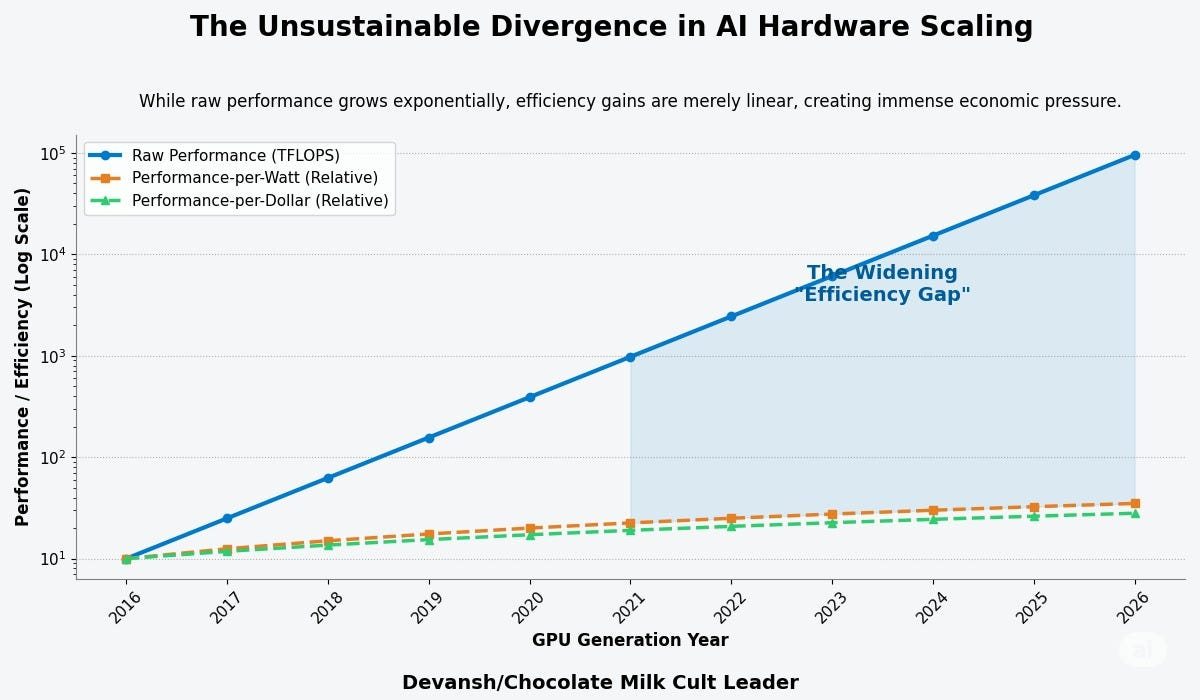
For much of the past decade, the strategy for increasing AI compute capacity was straightforward: deploy more, and more powerful, Graphics Processing Units (GPUs). This approach, while effective, has created a new set of challenges that are becoming untenable. We’re now grappling with divergence between raw performance scaling and efficiency scaling. While the computational power of successive GPU generations has grown exponentially, the improvements in performance-per-watt and performance-per-dollar have not kept pace (more on these metrics to come).
Take power. NVIDIA’s Blackwell B200 is consuming more energy than entire buildings. In such a case, Air cooling isn’t viable anymore — liquid loops are becoming mandatory. The CapEx is dwarfed by the OpEx, and TCO becomes a non-linear function of heat, not just compute.
Then there’s memory. Huge chunks of enterprise compute sits idle, locked to the CPUs that own it. We’re over-provisioning at every layer just to make utilization tolerable.
All this effort, and yet we can’t even really enjoy the fruits of our labor long term. The current GPU system performance is optimized for matrix multiplications — the sweet spot for Transformer training. It does a lot of these in parallel. That’s great for simplistic computations (like MatMul with full matrices). But that same rigidity makes it inefficient for anything that deviates: sequential operations, conditional logic, sparse inference. This is one of the reasons that the US government is heavily exploring other kinds of chips and computational processors, as we discussed here.
This is the specialization trap: tuning for today’s dominant workload at the expense of flexibility. It maximizes short-term throughput while increasing the risk of systemic fragility. One architectural shift — one model class that diverges from the Transformer mold — and half the stack loses relevance overnight.
A brave new world requires a new standard of judgment. Let’s look at the metrics we shall use to be our new law.
1.2 The New TCO Paradigm: Performance-per-Watt and Performance-per-Dollar as Key Metrics
While raw performance, often measured in floating-point operations per second (FLOPS), remains an important specification, it is no longer the sole determinant of value. Instead, sophisticated buyers, particularly hyperscale cloud providers and large enterprises, now prioritize more holistic business metrics:
Performance-per-watt (because datacenter power is now the constraint),
Performance-per-dollar (because at-scale inference eats margin), and
TCO under sustained load, not just burst performance.
That’s where NVIDIA’s challengers have found their angle.
Google’s TPUs routinely show 2–3x better performance-per-watt than comparable GPUs. Similarly, Amazon’s Trainium2 is priced to undercut GPU-based instances by 30–40%, especially for high-volume workloads. These aren’t “better chips” — they’re chips designed for a different game: sustained, predictable, low-margin inference at massive scale.
And that’s the key point: it’s no longer a race to the highest peak performance. It’s a cost optimization trench war — hardware CapEx, cooling OpEx, software efficiency, and platform integration all compounding across millions of daily inferences.
The battleground has changed. Most incumbents haven’t noticed.
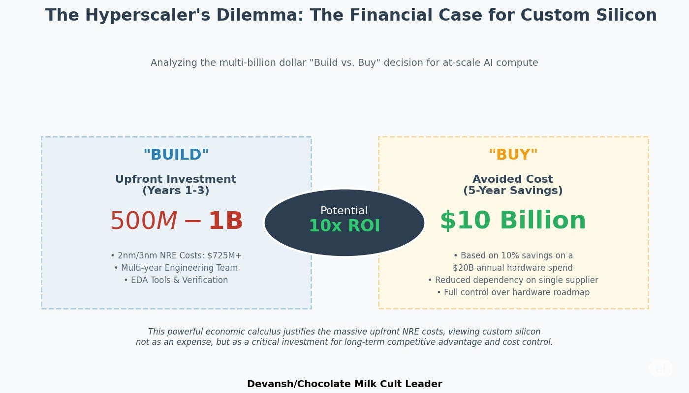
1.3 The Hyperscaler’s Dilemma: Re-evaluating the “Build vs. Buy” Equation in the Blackwell Era
Blackwell is a technical triumph. The DGX B200 system — eight B200s stitched together — is projected to deliver 15x the inference performance of the previous-gen DGX H100. For cutting-edge model training, it’s indispensable.
But the economics break on contact with scale.
Analyst estimates place the price of a single GB200 “superchip” (combining two B200 GPUs with a Grace CPU) in the range of $60,000 to $70,000. This high unit cost, coupled with the aforementioned 1,000W+ power consumption, reinforces the long-term strategic and financial logic for hyperscalers to “build” their own custom silicon.
To see if this is worth it, let’s do some math. As one might expect, the upfront investment required for a custom chip program is immense. Non-Recurring Engineering (NRE) costs for designing a chip on an advanced 3nm process node are formidable, with the mask set alone costing between $30 million and $50 million.
Furthermore, The total design cost for a leading-edge 2nm chip can approach $725 million.
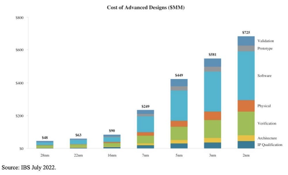
When factoring in the multi-year costs of a large engineering team, a hyperscaler’s total investment in a new chip generation can easily fall in the $500 million to $1 billion range.
Custom silicon — Google’s TPUs, AWS’s Trainium, Microsoft’s Maia — gives them control over:
Architecture (tuned for their real workloads),
Cost (no margin handed to NVIDIA),
Integration (tight coupling with their own software stacks), and
Roadmap (no dependency on third-party release cycles).
The numbers back it. A $1B investment into a custom chip program yields $10B in savings over 5 years if it cuts GPU spending by just 10%. That’s a 10x ROI. Not hypothetical. That’s the real math.
This dynamic creates a strategic challenge for NVIDIA. To defend its market share in the high-volume inference market against custom ASICs and AMD, it would need to compete aggressively on price, likely by lowering margins on its older hardware. Doing so, however, would risk cannibalizing sales of its newer, higher-margin products and compressing the overall profitability that its valuation is built upon.
Sucks to be daddy Jensen. But it’s a vibe for the rest of us. Let’s look at how this changes the game for hardware.
Section 2: The Hardware Revolution
The AI stack is no longer scaling vertically. It’s refactoring laterally. Specialized silicon, disaggregated memory, and optical I/O aren’t fringe R&D bets anymore — they’re converging into a new infrastructure regime.
The old system — throw more GPU at it — is collapsing under its own weight. What replaces it is a co-evolving triangle of technologies, each solving for the other’s constraints. This section outlines the hardware layer’s three core investment theses, and why winning this era will require seeing the stack as an interdependent chain, not a menu of options.
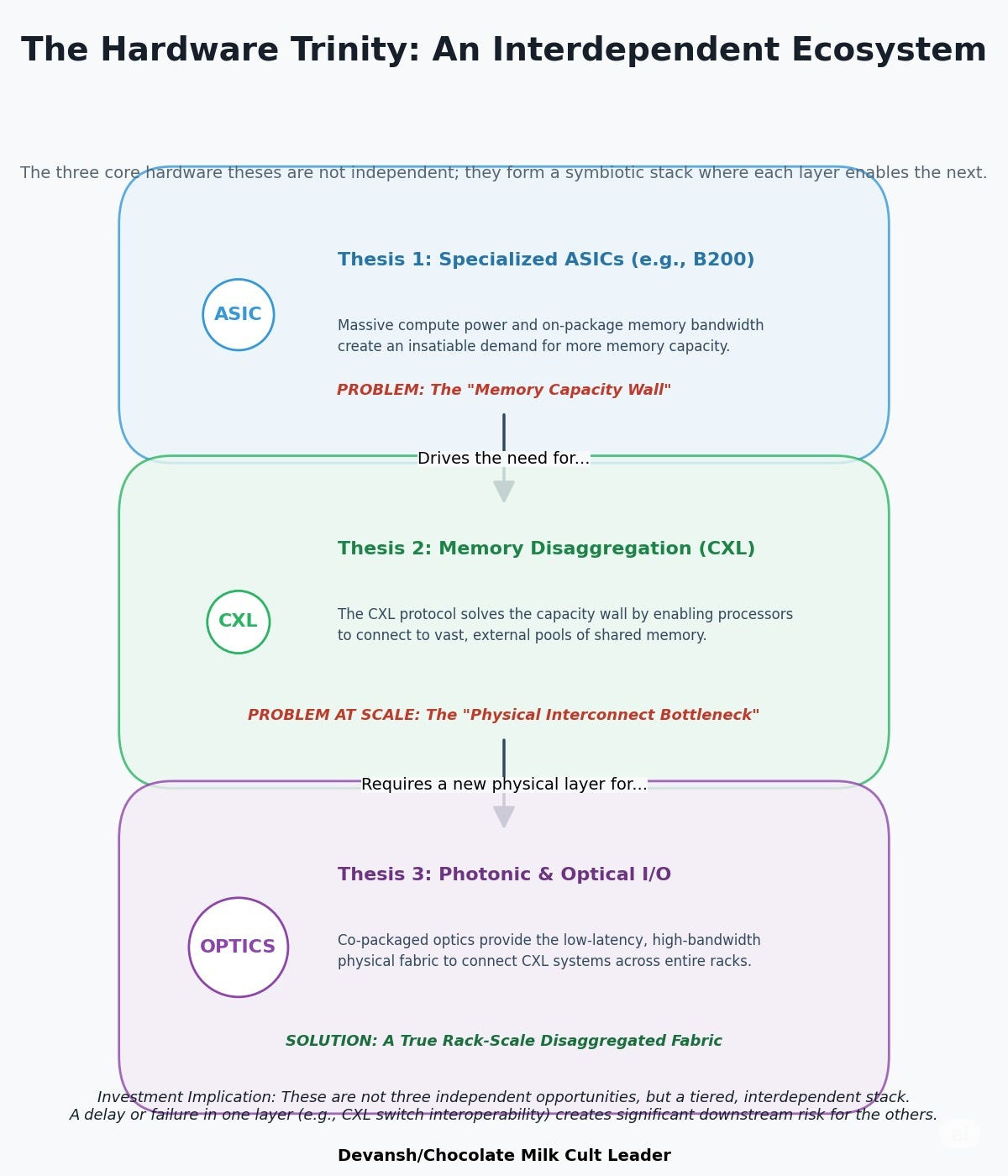
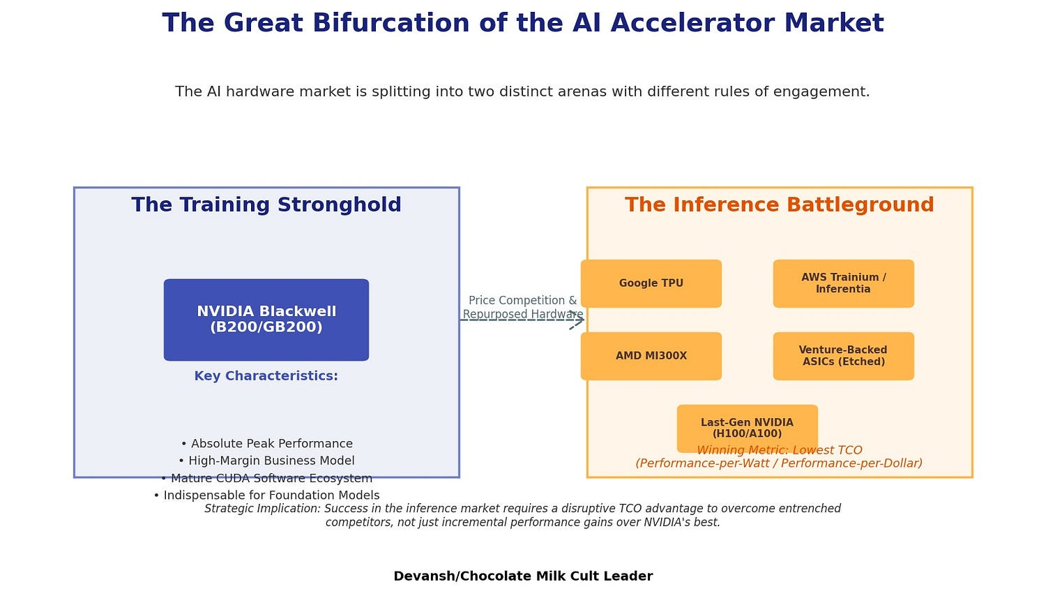
2.1 Specialized Silicon: Vertical Efficiency Over Horizontal Flexibility
General-purpose compute is being priced out of the stack. Specialized ASICs are taking its place — not because they’re faster in absolute terms, but because they’re architecturally aligned with how AI is actually run at scale.
Let’s repeat some information from the previous section, to ensure that we are following along on the important ideas. Skip section 2.1 if you took detailed notes in the last section. Keep reading if you want to get more detailed financial numbers on specialized vs general silicon.
2.1.1 NVIDIA Blackwell: The Endgame for General-Purpose
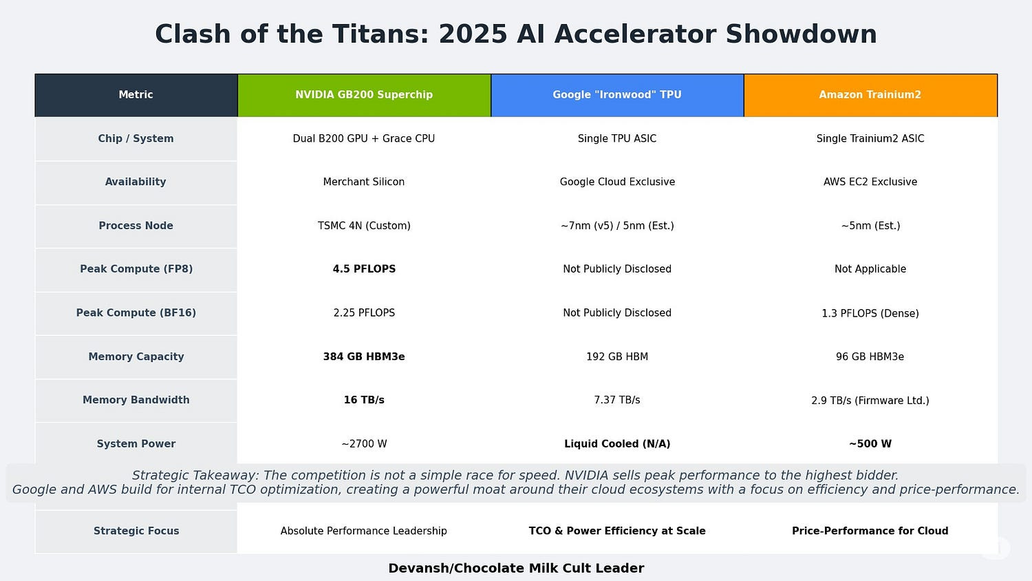
NVIDIA’s Blackwell (B200) is the current apex: dual-die, 208B transistors, 8 TB/s bandwidth, 1,000W+ TDP. The GB200 superchip pairs two B200s with a Grace CPU and sells for ~$60,000–70,000. It dominates training and high-performance inference — on paper.
But in practice, Blackwell signals a ceiling. Its thermal footprint demands full liquid cooling. Its energy draw reshapes data center design. And while it outperforms, it doesn’t transform: it’s still locked to the matmul-heavy, batch-friendly architecture of Transformers.
In short: Blackwell wins the past. It does not define the next decade.
2.1.2 The Hyperscaler Response: Vertical Integration at Scale
Google and Amazon aren’t chasing NVIDIA. They’re defecting from the entire model.
TPU Ironwood delivers 192 GB HBM, 7.37 TB/s bandwidth, and up to 5x power efficiency over H100s — built purely for Google’s stack.
Trainium2 hits 667 TFLOPS BF16 at 500W with pricing aimed at undercutting NVIDIA by 30–40%. It’s optimized for Mixture-of-Experts and bandwidth-constrained inference.
These aren’t just chips. They’re control points. Neither is sold as merchant silicon. That’s the point: they’re instruments of margin protection, stack ownership, and workload-specific optimization.
This is the hyperscaler thesis: own your architecture, your economics, and your roadmap. Stop renting scale from someone else.
2.1.3 The Venture Window: Narrow, But Not Closed
Startups like Etched and Lightmatter are going ultra-narrow:
Etched is hardwiring the Transformer into silicon for an order-of-magnitude TCO cut.
Lightmatter is building photonic-adjacent ASICs optimized for hybrid workloads.
But the bar is brutal. It’s not enough to beat NVIDIA on perf-per-watt. You have to overcome CUDA’s moat, survive long hyperscaler sales cycles, and offer a 10x TCO delta against hardware that’s already being discounted downstream.
Most won’t make it. But the one that does won’t just sell chips — it will rewrite the cost of inference globally.
2.1.4 At-Scale Inference Economics: A TCO Kill Shot
Take diffusion inference at 1,000 images/sec as a baseline:
On-prem B200s (167 units):
CapEx: $6.68M
Power OpEx (3 years): $658K
Total 3-year TCO: $7.34M

AWS Inferentia2 (1,205 instances):
Cloud OpEx: $24.05M
Total 3-year TCO: $24.05M

That’s a 70% reduction in TCO by owning optimized silicon. At hyperscaler scale, that delta compounds into billions. Every architectural choice now gets benchmarked not on throughput, but on whether it clears that cost wall.
2.1.5 Hyperscaler ROI: The $10B Reason to Go Vertical
Custom silicon programs aren’t just viable. They’re optimal.
NRE + team costs: $500M–$1B over 3 years.
GPU budget baseline: $20B annually.
10% efficiency gain = $2B saved/year = 10x ROI over 5 years.
One need look no further than how enthusiastically OpenAI has been investing in their chips, including stealing members of Google’s hardware division, to see how organizations that hit a certain scale end up inevitably needing chips.
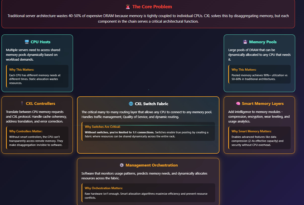
2.2 CXL: The Unlock for Memory-Limited Silicon
As ASICs get faster, they hit a new wall: they can’t feed themselves. The bottleneck isn’t compute — it’s memory capacity and bandwidth. That’s where Compute Express Link (CXL) enters the stack. It’s a high-bandwidth, low-latency standard that allows memory to be disaggregated from the CPU and put into a shared pool. Instead of overprovisioning every server, you treat memory as a fungible, allocatable resource.
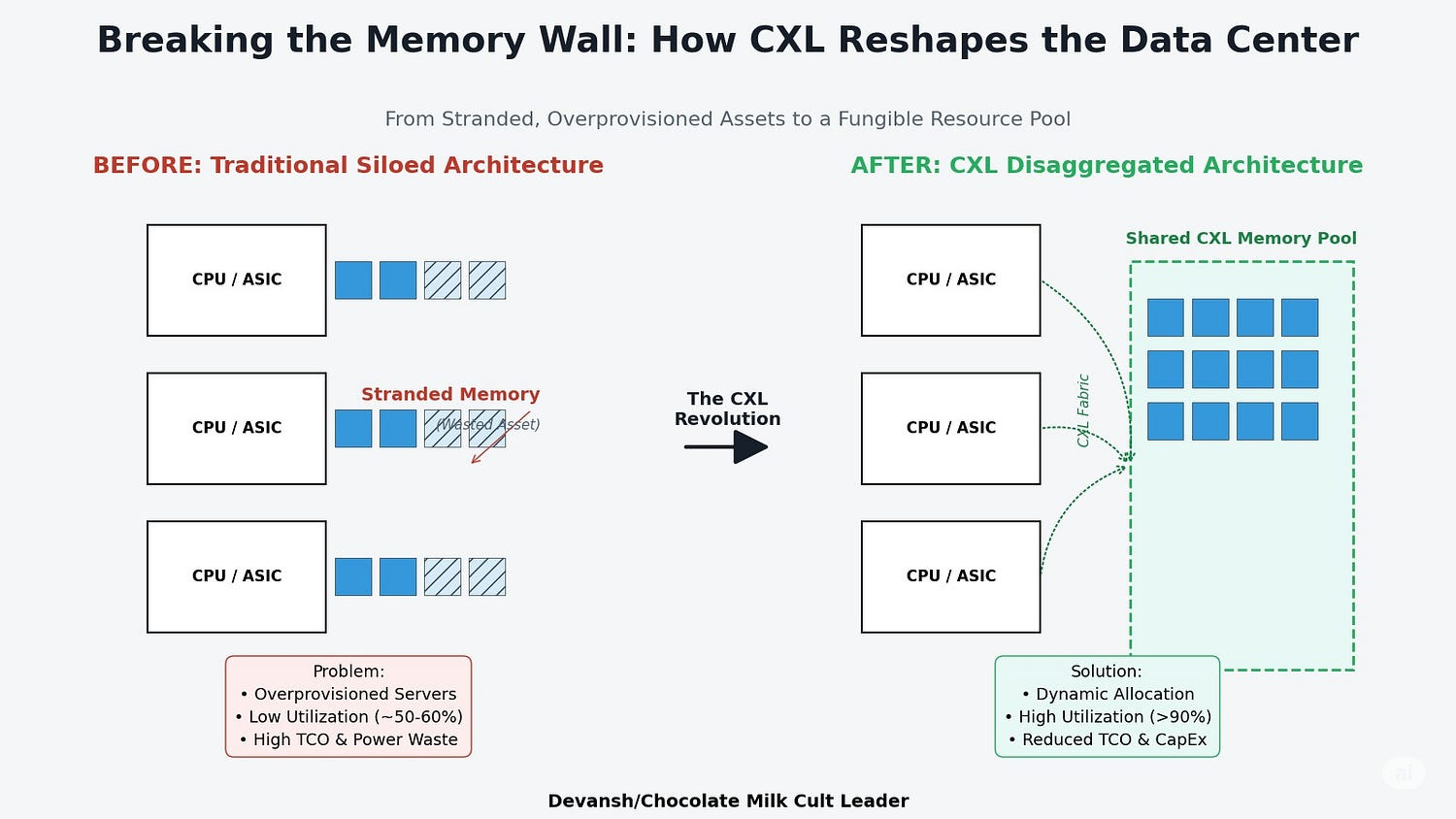
2.2.1 Breaking the Memory Lock-In
Traditional servers chain DRAM to CPUs. That means memory is stranded and utilization caps at ~50–60%. CXL breaks that tether. It turns memory into a dynamic, shared pool addressable by any processor on the fabric.
From 391 servers (non-CXL) → 200 servers (CXL) to provision 100TB RAM.
25% memory cost reduction.
Up to 30% overall 3-year TCO reduction.
This isn’t just a better bus. It’s a structural re-architecture of memory’s role in the system.
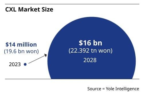
2.2.2 Market Maturity
The roadmap:
2023–25: Memory Expansion (CXL 1.1/2.0)
2025–27: Pooling & switching (CXL 3.x)
2028+: Rack-scale disaggregation standard
From $0 to 16B by 2028. The shift is not speculative — it’s already underway.
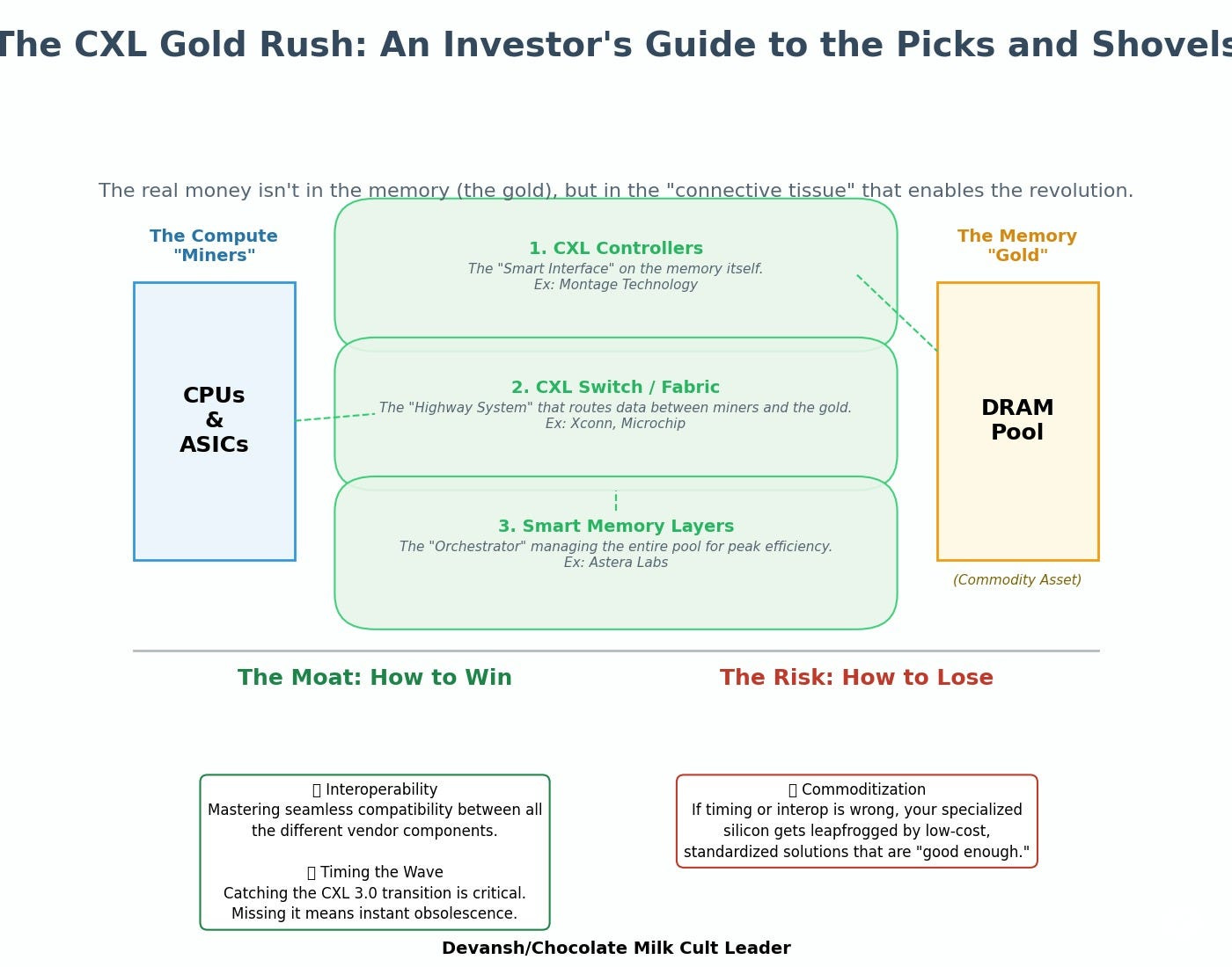
2.2.3 Where to Invest
The winners won’t be DRAM manufacturers — they’ll be the connective tissue:
CXL Controllers (Montage)
Switch/Fabric Players (Xconn, Microchip)
Smart Memory Layers (Astera Labs)
This is a classic picks-and-shovels play. But timing is everything. The moat is interoperability and timing the shift to CXL 3.0 just right. Miss the window, and your silicon gets leapfrogged by commodity standardization.
2.3 The Long-Term Disruptor: Photonics and the Physical Limits of Copper
To understand why photonics matters, forget the hype and start with physics.
Every modern AI system relies on moving massive amounts of data — between memory and compute, between chips, between servers. Right now, nearly all of that movement happens through copper wires. It’s the backbone of the modern datacenter.
But copper is not magic. It has constraints:
It loses signal strength over distance.
It consumes increasing amounts of power as bandwidth rises.
It generates heat, which compounds with every generation.
And it takes up real physical space on boards and backplanes.
These limitations weren’t an issue when compute was mostly contained inside a server box. But the new AI stack doesn’t look like that anymore. Compute is being disaggregated — memory, processors, and accelerators are being pulled apart and recombined across entire racks. CXL enables this logically. But copper can’t keep up physically.
That’s where photonic systems come in.
Rather than transmitting data using electrical signals through copper, photonics transmits information using light. Light travels faster. It doesn’t generate heat through resistance. It doesn’t lose signal strength over distance. And it can carry significantly more data in a tighter form factor.
But “photonic AI” is not one technology. It splits into two fundamentally different strategies — each attacking a different pressure point in the stack.
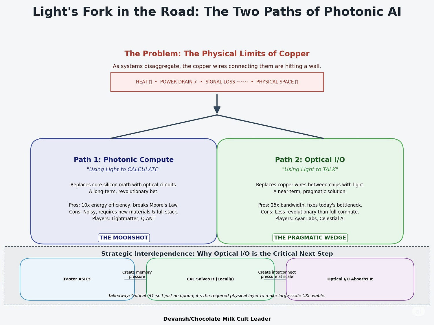
2.3.1 Photonic Compute: Replacing the Core Math
The first approach is the most ambitious: use light not just to transmit data, but to compute with it.
Right now, nearly all AI math — matrix multiplications, convolutions, vector ops — happens inside silicon chips. Those operations are handled by electrons passing through transistors in CPUs, GPUs, or ASICs. But those electrons generate heat. They have latency. They consume power. And you can only cram so many into a chip before you run into hard limits.
Photonic compute flips that paradigm. Instead of electrons, it uses photons — particles of light — to do the math directly.
How?
In short: by passing light through a network of tiny optical components — modulators, waveguides, phase shifters — that perform mathematical transformations as the light travels. These transformations correspond to the kinds of linear algebra operations AI models rely on.
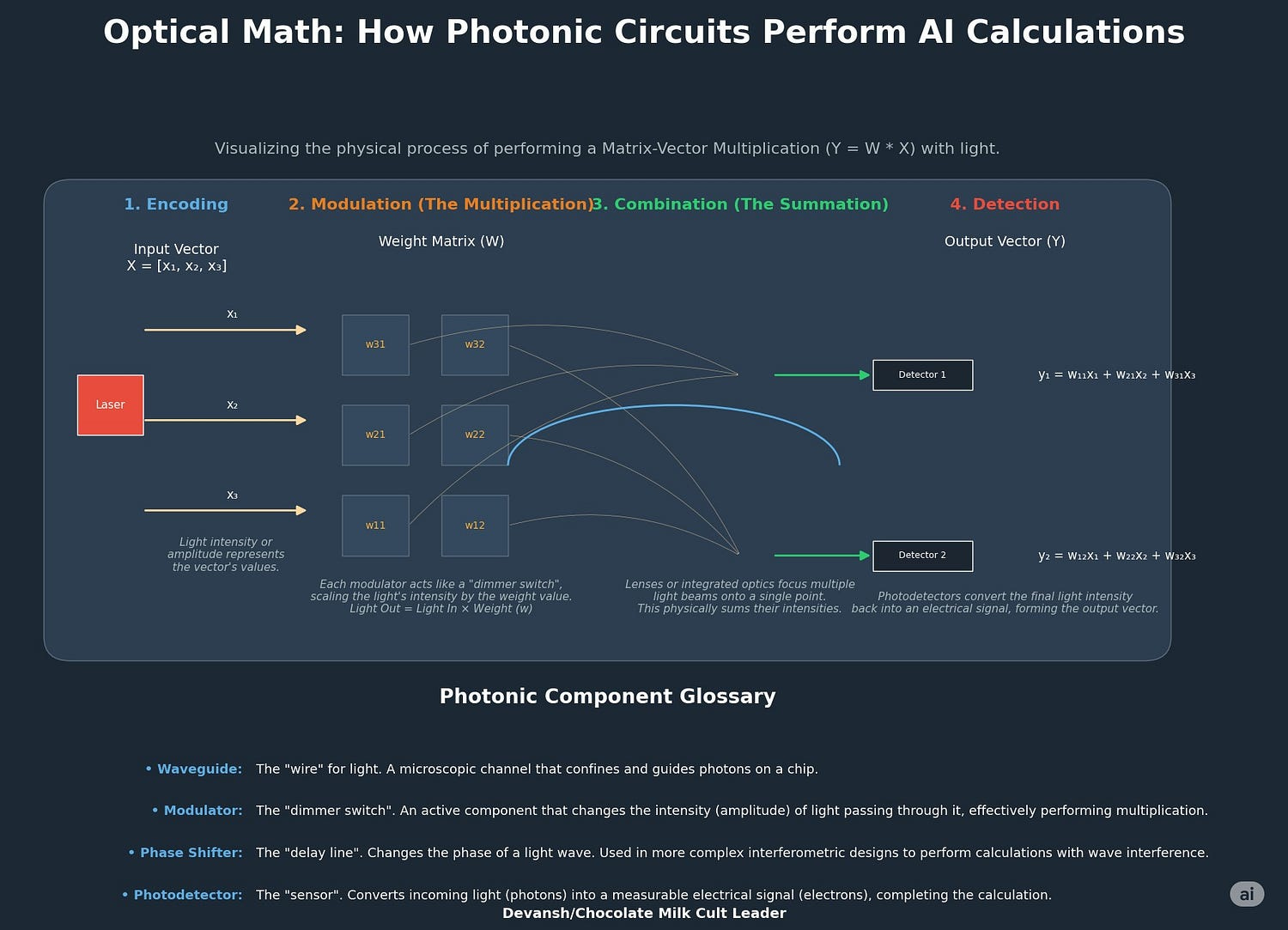
Startups like Lightmatter and Q.ANT are pursuing this path:
Lightmatter’s Envise processor performs matrix-vector multiplications optically, claiming up to 10x speed plus energy efficiency over traditional silicon accelerators.
The upside is enormous: ultra-low energy use, high bandwidth, and the potential for compute throughput that breaks free of today’s silicon ceilings.
But so are the challenges:
Light-based calculations can be noisy — tiny fluctuations in intensity affect precision.
You need exotic materials (like indium phosphide) that don’t always integrate well with existing chip fabs.
And most critically, it requires a completely new software and hardware stack — you’re not just swapping chips, you’re reinventing the platform.
This path isn’t about the next 2 years. It’s about what happens when Moore’s Law fully expires and silicon can’t scale. It’s not a tactical solution — it’s a bally bet at tech that reads like a scifi fantasy. And I’m a huge sucker for this kind of work.
The second — and much more immediate — use of photonics doesn’t change the way we compute. It changes how compute systems talk to each other.
2.3.2 Optical I/O: Fixing the Interconnect Bottleneck
Right now, data moves between chips (CPU↔GPU, GPU↔Memory) through electrical interconnects: specialized circuits like SerDes (serializer/deserializer blocks) that translate and route bits. These wires are fast — but they’re failing to keep up.
As AI systems grow, interconnect becomes the bottleneck:
GPUs can process more data than the wires can deliver.
Disaggregated memory architectures (like CXL) require high-bandwidth, low-latency communication between multiple boxes or racks.
Every extra inch of wire increases power draw, latency, and the risk of signal degradation.
Optical I/O solves this. Instead of sending electrical pulses through metal, it sends light through fiber or integrated photonic waveguides — often co-packaged right next to the chip.
This is the near-term wedge where companies like Ayar Labs and Celestial AI are moving fast:
Ayar Labs’ TeraPHY optical chiplets deliver up to 8 terabits per second of bandwidth with under 5 nanoseconds of latency — all at a fraction of the power consumption of electrical SerDes.
Celestial AI’s Photonic Fabric claims up to 25x bandwidth and 10x energy savings over copper-based alternatives.
These aren’t science projects. They’re already being validated in hyperscale environments. And unlike photonic compute, optical I/O doesn’t require the rest of the system to change. It just replaces the part of the stack that’s already showing cracks.
And most importantly: CXL depends on this.
You can’t have dynamic memory pools spread across a rack — or across racks — if your interconnect can’t support it. Copper won’t scale there. Light will.
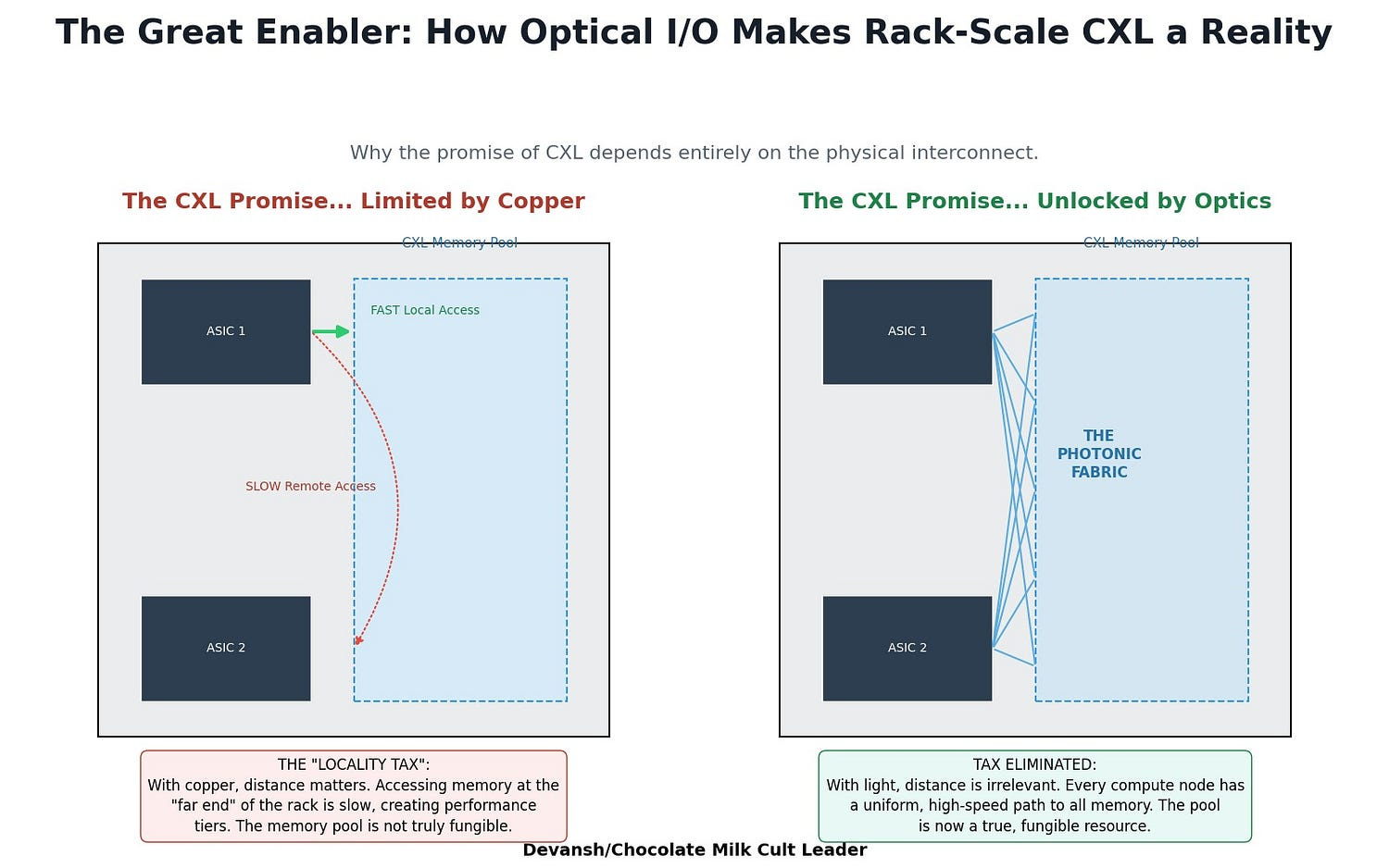
2.3.3 Strategic Interdependence: Why These Layers Are Chained — and Where That Leads
This triad — ASICs, CXL, Optical I/O — is not a buffet of upgrade options. It’s a dependency chain. And that has consequences.
Once you start the chain, you can’t stop halfway.
If you adopt faster, memory-starved ASICs, you’re forced to adopt CXL to avoid underutilization. Once you adopt CXL, and your memory fabric stretches beyond the box, Optical I/O becomes the only viable physical layer. This is not just a technical relationship — it’s a capital commitment and an organizational realignment.
The implications are long-range and structural:
1. Timeline Compression for Strategic Buyers
CXL is not a future tech. It’s already shipping in AMD Genoa and Intel Granite Rapids. Memory expansion is underway.
By 2027–2029, CXL 3.0-based memory pooling becomes feasible at scale. That’s also the window where data centers hit peak Blackwell-induced power draw.
At the same time, Optical I/O will no longer be optional. The moment you stretch pooled memory beyond a single chassis, you exceed what copper can do without a power and latency penalty. Expect full-stack hyperscalers — AWS, Google, Meta — to shift into production deployment between 2027–2029 (I expect to see successful early deployments by next year), especially in AI-dedicated buildouts.
Anyone who delays adoption beyond 2031 is not “saving cost” — they’re taking a long position on architectural obsolescence.
2. Infrastructural Path Dependency
This is not a “swap and test” stack. Once a hyperscaler moves to a photonic interconnect layer:
Every ASIC that wants to plug in needs to be compatible
Memory vendors must support CXL protocols and optical uplinks
Datacenter orchestration software must become hardware-aware: NUMA topologies, near/far memory classification, dynamic pooling logic, etc.
This creates lock-in through physics. Not software. Not licensing. But thermals, bandwidth ceilings, and rack layout realities.
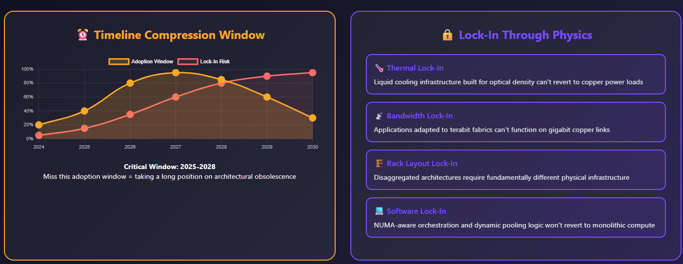
Once a vendor standardizes on photonic I/O and pooled memory, switching away becomes not just costly — it’s architecturally impossible without a full rebuild. Seen from this perspective, investing in any one layer is not about upside — it’s about securing presence across the chain before the interlocks calcify.
3. The Post-GPU Stack as a National Asset
As we’ve already discussed in past articles and AI market reports, hardware is now treated like a strategic asset for geopolitical reasons. By 2031, the US government wants to unravel huge parts of the GPU dependency by investing in more kinds of systems. Make no mistake, the reasons behind this are as strategic as they are scientific/technical.
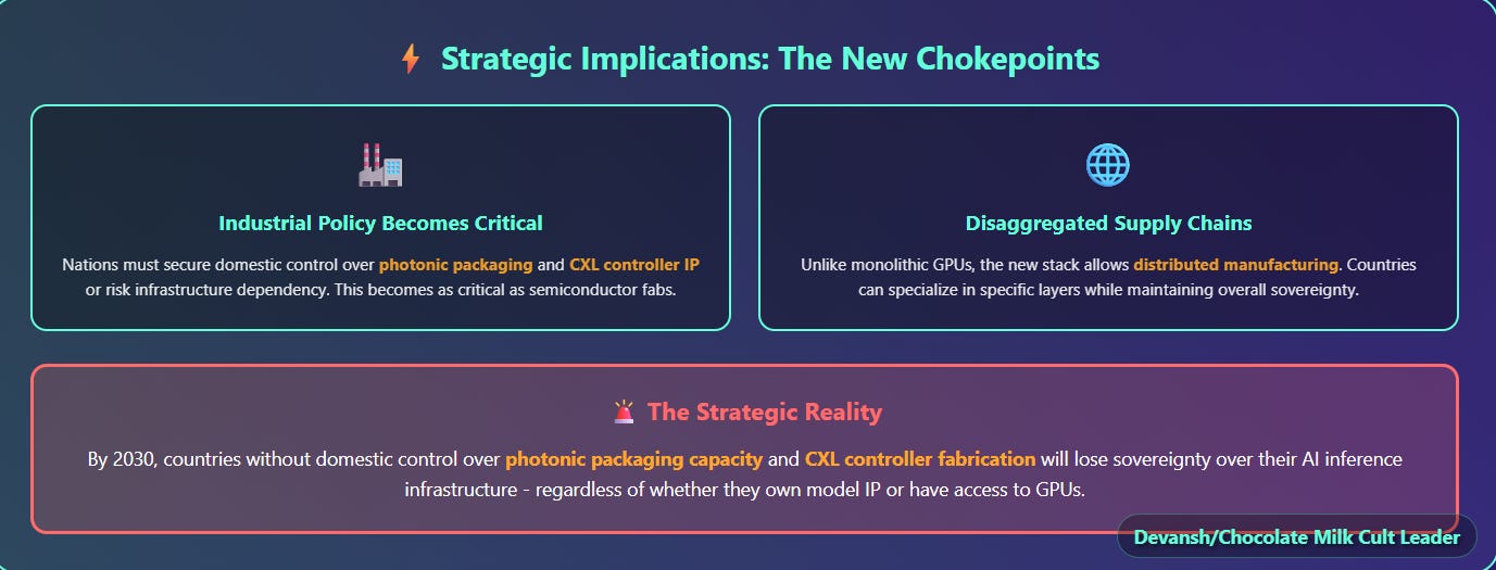
Strategic autonomy requires compute autonomy. Once this chain is mature, national and sovereign datacenter programs will no longer just compete on access to GPUs — they’ll compete on control over:
Photonic I/O fabrication capacity
CXL controller IP and licensing
In-house or locally built ASIC architectures
This stack doesn’t just rebalance industry dynamics. It fractures the current monopoly state held by GPU vendors and opens the door for regional or vertical challengers.
It also opens the door to industrial policy. Countries without domestic CXL memory controller fabs or photonic packaging capacity will lose control over their AI inference infrastructure — regardless of whether they have model IP or not.
4. The Strategic Bet: The Stack Won’t Recombine
One final implication: this is a one-way replatforming.
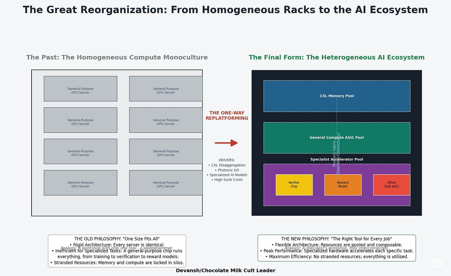
There will be no return to monolithic compute. Once memory is disaggregated, it stays disaggregated. Once photonic I/O stretches compute across racks, software orchestration will adapt accordingly — and that software stack won’t revert. The cost advantages of flexible, pooled, ultra-dense architectures are too great. Especially when you consider that SLMs will require custom verifiers, special rewards functions, and other vertical optimizations to hit peak performance. This changes your rack from homogeneous (lots of the same kinds of chips) to heterogeneous (multiple kinds of chips/systems that handle specialized tasks).
The investment + benefits of this approach ensure that this approach will generate a lot of momentum, driving up switching costs significantly. And this creates long-term recurring revenue and ecosystem lock-in.
Long-Term Strategic Implications:
The End of the Monolithic Server: The fundamental unit of compute is shifting from the “server box” to the “disaggregated rack.” This kills the business model of traditional server OEMs who sell integrated boxes and creates a massive opening for players who can build and manage these new, complex, heterogeneous systems.
The Rise of the “Fabric Baron”: As value moves from the individual components (CPU, memory) to the interconnect that ties them together, a new kingmaker emerges: the owner of the dominant optical fabric. This is the strategic endgame for companies in the photonics space — to become the “Broadcom of light.”
The Software Choke Point: This entire hardware revolution creates a terrifying new problem. A rack full of disaggregated, specialized hardware is an inert pile of silicon without a new kind of software to orchestrate it. The current generation of cloud orchestrators like Kubernetes is hardware-agnostic and fundamentally unprepared for this world.
This hardware is the foundation, but it is a body without a brain. It solves the problems of physics and economics only to create a new, even more complex challenge at the software layer. Controlling the hardware is one thing; controlling what it does is the ultimate source of power.
And that is where we will pick up in Part 2. For now, let’s end this article.
Conclusion
We’ve now entered the post-GPU era — not because GPUs have disappeared, but because their economics no longer govern the architecture. The new substrate is taking shape: specialized silicon, disaggregated memory, optical interconnects. It’s not more of the same — it’s a complete realignment of how compute, memory, and bandwidth relate to one another.
But physical infrastructure is only half the battle.
What happens when this new stack runs into real-world constraints?
When pooled memory requires new classes of orchestration software
When photonic systems create vendor lock-in at the physical layer
When sovereign data centers demand transparency, control, and local manufacturability
When every generation of accelerators widens the gap between what we can compute and what we can afford to manage
The technical direction is clear. But the operational, regulatory, and geopolitical pressures are just starting to show. And they’ll be just as defining as the hardware itself.
This is where Part II begins — moving up the stack to explore how compression, governance, talent, and dynamic control systems will — or won’t — adapt to the new substrate we’ve just mapped.
The hardware has shifted. Now we find out if the software, and the institutions that depend on it, can follow.
Thank you for being here, and I hope you have a wonderful day.
I like hard(ware) things,
Dev <3
If you liked this article and wish to share it, please refer to the following guidelines.
That is it for this piece. I appreciate your time. As always, if you’re interested in working with me or checking out my other work, my links will be at the end of this email/post. And if you found value in this write-up, I would appreciate you sharing it with more people. It is word-of-mouth referrals like yours that help me grow. The best way to share testimonials is to share articles and tag me in your post so I can see/share it.

Reach out to me
Use the links below to check out my other content, learn more about tutoring, reach out to me about projects, or just to say hi.
Small Snippets about Tech, AI and Machine Learning over here
AI Newsletter- https://artificialintelligencemadesimple.substack.com/
My grandma’s favorite Tech Newsletter- https://codinginterviewsmadesimple.substack.com/
My (imaginary) sister’s favorite MLOps Podcast-
Check out my other articles on Medium. : https://rb.gy/zn1aiu
My YouTube: https://rb.gy/88iwdd
Reach out to me on LinkedIn. Let’s connect: https://rb.gy/m5ok2y
My Instagram: https://rb.gy/gmvuy9
My Twitter: https://twitter.com/Machine01776819
So we've just come to some fairly dramatic conclusions here, correct?
Does anyone want to offer an opposing perspective? Does anyone see any significant holes in his arguments or in his thesis? (Many thinks to dyb5785 for his framework- and AI-based analyis and elucidation.)
I loved the depth you brought to this topic. But reading it, I kept wondering... It seems like the big players will have no choice but to jump early or risk being locked out of viable supply chains. But how does a midsize company even plan for that?