AI x Computing Chips: How to Use Artificial Intelligence to Design Better Chips [Breakdowns]
Faster (months --> hours) and Better (6.2%) Chip Design using Reinforcement Learning and Graphs
Hey, it’s Devansh 👋👋
In my series Breakdowns, I go through complicated literature on Machine Learning to extract the most valuable insights. Expect concise, jargon-free, but still useful analysis aimed at helping you understand the intricacies of Cutting-Edge AI Research and the applications of Deep Learning at the highest level.
I put a lot of effort into creating work that is informative, useful, and independent from undue influence. If you’d like to support my writing, please consider becoming a paid subscriber to this newsletter. Doing so helps me put more effort into writing/research, reach more people, and supports my crippling chocolate milk addiction. Help me democratize the most important ideas in AI Research and Engineering to over 100K readers weekly. Many companies have a learning budget that you can expense this newsletter to. You can use the following for an email template to request reimbursement for your subscription.
PS- We follow a “pay what you can” model, which allows you to support within your means, and support my mission of providing high-quality technical education to everyone for less than the price of a cup of coffee. Check out this post for more details and to find a plan that works for you.
When I started researching Google’s use of AI in Quantum Computing for their Willow Chip, I became curious about the use of AI in improving Computing Chips in general. That’s how I found the publications- “How AlphaChip transformed computer chip design” and “A graph placement methodology for fast chip design”.
The publications talk about Google’s Open Source AI- AlphaChip- that has dramatically sped up chip design. “AlphaChip was one of the first reinforcement learning approaches used to solve a real-world engineering problem. It generates superhuman or comparable chip layouts in hours, rather than taking weeks or months of human effort, and its layouts are used in chips all over the world, from data centers to mobile phones.” Its results are remarkable enough that it’s used in production, both internally by Google-

and externally-
Other organizations have adopted our approach and built on it. For example, MediaTek, a leading global chipmaker, extended AlphaChip to accelerate development of their most advanced chips, while improving power, performance, and area
To contextualize the importance of this, let’s do some quick back-of-the-hand calculations (please feel free to correct me if I’m making any mistakes/bad assumptions here)-
Cost savings: Assuming AlphaChip reduces chip design time from 6 months to 1 week, and considering an average chip design team of 50 engineers with an annual salary of $150,000 each:
Potential savings per chip design: (150,000*50*(6/12–1/52))≈$ 3,605,769 (3.6 Million USD).
Performance improvements: If AlphaChip designs are 20% more power-efficient, this could translate to hundreds of millions of dollars saved for large power centers.
Market adoption: “The global electronic design automation was valued at USD 14.5 billion in 2022 and is estimated to reach USD 26.2 billion by 2028, registering a CAGR of 9.8% during the forecast period.” If AlphaChip and the Cell Juniors it spawns can be integrated into even 10% of this market (shouldn’t be difficult given that this is Google we’re talking about), that’s a value of 1.4–2.6 Billion USD to be captured. Google’s release of AC as an Open Source Project is a strategically brilliant move here (your regular reminder that Open Source is much much more than just a loss leader, which we explained here)-
Those numbers go up as edge computing, specialized Chips, and tech penetration become more common. It’s also worth noting that good technology often increases it’s domain’s market share (the way ChatGPT increased budgets/adoption for AI, even in techniques that didn’t use NLP).
I’m going to skip our usual table of impacts here since most of the impact of this specific research is going to be commercial. However, I think the spirit of this research (using RL for better planning and forecasts) could have interesting impacts in other use cases that can help with energy efficiency, new simulations, city design etc. In that context, this could encourage more interest in engineering with Reinforcement Learning (especially when combined with other interesting RL work like Scalable RL with Mixture of Experts)- leading to breakthroughs in those other fields.
In addition to the immediate impact on chip floorplanning, the ability of our method to generalize and quickly generate high-quality solutions has major implications, unlocking opportunities for co-optimization with earlier stages of the chip design process. Large-scale architectural explorations were previously impossible, because it took months of human effort to accurately evaluate a given architectural candidate. However, modifying the architectural design can have an outsized impact on performance, and would facilitate full automation of the chip design process. Automating and accelerating the chip design process can also enable co-design of AI and hardware, yielding high-performance chips customized to important workloads, such as autonomous vehicles, medical devices and data centres.
-I don’t know enough about hardware design to make any strong assertions, but this seems a bit exagerrated (I don’t know if chip quality is the limiting factor in these cases). However, this looked interesting enough for me to flag.
If all that sounds interesting, let’s break down the research.
PS- AI Made Simple is about to hit its 2nd birthday. We will be hosting an AMA (ask me anything) to celebrate this. You can ask your questions in the comments, message me on any of the social media links, reply to this email, or drop any questions you have in this anonymous Google Form- https://docs.google.com/forms/d/1RkIJ6CIO1w7K77tt0krCGMjxrVp1tAqFy5_O2FSv80E/ (preferred).
Executive Highlights (TL;DR of the article)
To understand this research, we must first understand the existing methods and where they failed.
Background & Context
Chip floorplanning requires placing circuit components optimally while balancing power, timing, and area constraints. This process has become incredibly complex due to the exponential growth in the number of components on modern chips, rendering traditional methods inadequate for different reasons:
Partitioning-based methods: These divide the chip into smaller sections to make the problem manageable but sacrifice global optimization (components in different sections will influence each other- something that methods can struggle to model). Notably, poor early partitioning decisions can’t be fixed later and might also be fatal. I wonder if Supervised Learning to score states might be a valuable low-resolution filter to catch the bad partitions early.
Hill-climbing approaches: These iteratively make small improvements but get stuck in local optima and don’t scale to modern chips with billions of nodes.
Analytic solvers: While more sophisticated, these can only optimize differentiable functions, making them unsuitable for critical metrics like routing congestion- when there are too many wires trying to pass through a small area on the chip, causing issues with performance power consumption and even make it impossible to complete the design.
These limitations, coupled with the exponential growth in chip complexity, have led to heavy reliance on human experts, who spend months iterating with electronic design automation (EDA) tools to produce viable layouts.
This is where RL might be hugely promising.
Why Deep RL is Promising
Chip placement naturally fits reinforcement learning because:
It’s sequential: Components are placed one at a time, with each decision affecting future possibilities.
It benefits from experience: Patterns and strategies learned from one design can transfer to others.
It handles non-differentiable objectives: RL can optimize for any reward signal, including complex manufacturing constraints.
It can learn general principles: Rather than solving each design from scratch, RL learns transferable placement strategies (similar to how RL helped AlphaGo learn strategy for Go, instead of simply picking up a set of moves).
It allows for exploration: RL can explore novel placement options that human designers might miss (same example as above).
RL is combined with some other heavy hitters to nail the universe cross-over that DC has been trying to pull off for years (Injustice is such an elite story, how have they not turned that into a best-selling movie/TV series yet?).

Let’s understand the players that make this super-team work.
Core Technical Innovations
Starting from a blank grid, AlphaChip places one circuit component at a time until it’s done placing all the components. It’s rewarded based on the quality of the final layout. AlphaChip utilizes a new type of graph neural network that focuses on the connections between chip components. This allows it to understand how different parts of a chip interact and apply that knowledge to new designs, effectively learning and improving with each chip layout it creates.
This relies on several components-
Edge-Based Graph Neural Network (Edge-GNN): Instead of just looking at individual components, this network focuses on relationships between components. This is crucial because component interactions (like wire lengths and signal timing) determine placement quality. Interestingly, the Edge-GNN is used not for predictions but as an encoder to create feature embeddings for the network prediction (shown in the image above). Seeing the focus on embeddings makes me very very happy.
Hierarchical Placement: Places large components (macros) first using RL, then handles smaller components with faster methods, making the problem tractable and improving our control on the outputs (it’s easier to control non Deep Learning methods).

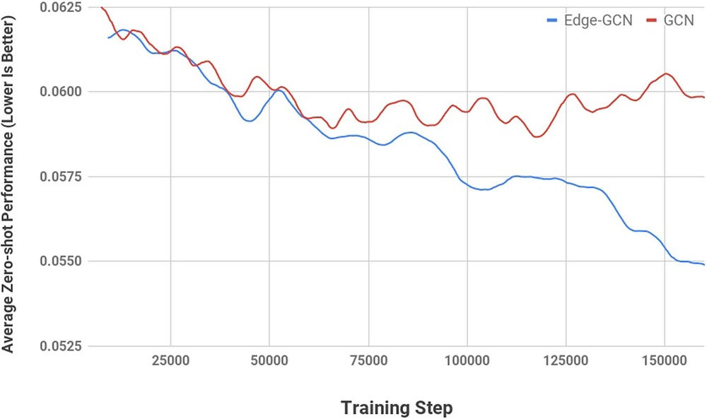
Transfer Learning: AC pre-trains on multiple chip designs to learn general placement principles, like keeping frequently communicating components close together. We can use the base-level pretraining or fine-tune further to optimize gains for specific setups. Based on the results below- zero-shot seems like it does a pretty good job- which is a good indication that the representations are robust.

Custom Reward Function: Balances multiple objectives (power, timing, area) while enforcing manufacturing constraints.
RL Training: Uses Proximal Policy Optimization (PPO) to effectively navigate the enormous state space and learn stable placement strategies.
Aside from this, there are following are the other aspects of this setup that I thought were interesting.
Other Highlights
Constraint Handling: Embeds constraints by masking out illegal placements, allowing the agent only to consider valid actions during training, which improves training efficiency.
The Computational Efficiency: “In terms of resource usage, for pre-training we used the same number of workers as blocks in the training dataset (for example, for the largest training set with 20 blocks, we pre-trained with 20 workers) and the pre-training runtime was 48 h. To generate the fine-tuning results in Table 1, our method ran on 16 workers for up to 6 h, but the runtime was often considerably lower owing to early stopping. For both pre-training and fine-tuning, a worker consists of an Nvidia Volta graphics processing unit (GPU) and 10 central processing units (CPUs), each with 2 GB of RAM. For the zero-shot mode (applying a pre-trained policy to a new netlist with no fine-tuning), we can generate a placement in less than a second on a single GPU.”
This is remarkably efficient compared to traditional approaches requiring months of human expert time-
We show that our method can generate chip floorplans that are comparable or superior to human experts in under six hours whereas humans take months to produce acceptable floorplans for modern accelerators. Our method has been used in production to design the next generation of Google TPU.
That was my tl;dr of the work. The rest of this article will cover the following-
How AlphaChip represents Chip floorplanning as a learning problem
How they handle multiple objectives and constraints to create a comprehensive learner.
A deep-dive on their AI implementation that creates generalized representations.
and more discussions on their results.
Keep reading if that interests you.
I put a lot of work into writing this newsletter. To do so, I rely on you for support. If a few more people choose to become paid subscribers, the Chocolate Milk Cult can continue to provide high-quality and accessible education and opportunities to anyone who needs it. If you think this mission is worth contributing to, please consider a premium subscription. You can do so for less than the cost of a Netflix Subscription (pay what you can here).
I provide various consulting and advisory services. If you‘d like to explore how we can work together, reach out to me through any of my socials over here or reply to this email.
How to encode Chip floorplanning as a learning problem
The core innovation of AlphaChip lies in its ability to transform the complex task of chip floorplanning into a problem that can be tackled by a reinforcement learning (RL) agent. Instead of relying on traditional, rule-based algorithms or manual human effort, AlphaChip approaches chip design as a sequential decision-making process. This means that the chip layout is not created all at once but rather one component at a time, with each placement decision influencing the subsequent ones.
The Benefits of Sequential Approaches
This sequential approach is crucial for several reasons:
Learning from Experience: The agent learns from the consequences of its past actions. Each placement affects the subsequent placements, and the agent learns to make decisions that lead to the best overall outcome.
Breaking Down Complexity: By placing components one at a time, the agent avoids the computational challenges of attempting to solve the entire placement problem simultaneously.
Dynamic Adaptation: The agent can adapt to the changing state of the environment, making informed decisions based on the current layout.
To pull this off, they rely on a classic-
Markov Decision Process Components
The floor planning is represented as an MDP. This is very common in RL setting so let’s understand it very quickly-
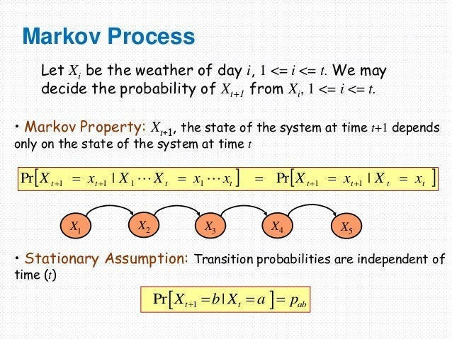
A Markovian Process is a type of stochastic (random) process where the future state of a system depends only on its current state, not on its entire history. The “memorylessness” of the process simplifies its modeling-
Imagine a Mario Game. As long as two different game instances have identical coins, powerups, health bars, locations, timers, and other stats- the journey you took to get to that point is irrelevant. Where you go/what you can do from that point on is also fixed, making those two points functionally identical- even if you took very different journeys to get there.
Markovian Processes are very cool b/c a lot of extremely complicated processes can be simplified into MPs.

From this foundation, we build Markov Decision Processes (MDPs) — the mathematical framework behind reinforcement learning. MDPs extend Markov Processes by adding 3 crucial elements:
Actions: An agent can make choices that influence state transitions
Rewards: Each state-action pair yields a reward signal
Discount Factor: Future rewards are worth less than immediate ones
For AlphaChip, this plays out as following-
States (st): “States encode information about the partial placement, including the netlist (adjacency matrix), node features (width, height, type), edge features (number of connections), current node (macro) to be placed, and metadata of the netlist graph (routing allocations, total number of wires, macros and standard cell clusters).
Actions are all possible locations (grid cells of the chip canvas) onto which the current macro can be placed without violating any hard constraints on density or blockages.
(3) State transitions define the probability distribution over next states, given a state and an action.
(4) Rewards are 0 for all actions except the last action, where the reward is a negative weighted sum of proxy wirelength, congestion and density, as described below.”
The reward function is particularly interesting. Let’s touch on it next.
“Our goal is to minimize PPA, subject to constraints on routing congestion and density. Our true reward is the output of a commercial EDA tool, including wirelength, routing congestion, density, power, timing and area. However, RL policies require 10,000s of examples to learn effectively, so it is critical that the reward function be fast to evaluate, ideally running in a few milliseconds. In order to be effective, these approximate reward functions must also be positively correlated with the true reward. Therefore, a component of our cost is wirelength, because it is not only much cheaper to evaluate, but also correlates with power and performance (timing).
To combine multiple objectives into a single reward function that can be optimized, we take the weighted sum of proxy wirelength, congestion and density, where the weights can be used to explore the trade-off between these metrics. While we treat congestion as a soft constraint (that is, lower congestion improves the reward function), we treat density as a hard constraint, masking out actions (grid cells to place nodes onto) the density of which exceeds the target density.”
How AlphaChip Handles Multiple Objectives
A key challenge in chip floorplanning is the need to optimize multiple, often competing, objectives while adhering to strict constraints. AlphaChip addresses this challenge through a carefully designed reward function and a novel approach to constraint handling.
The Reward Function Architecture
In reinforcement learning, the reward function is the compass that guides the agent towards desirable outcomes. In AlphaChip, the reward function is not a single metric but a combination of several key objectives, reflecting the complex trade-offs involved in chip design.
AlphaChip uses a sparse reward structure where all intermediate rewards are zero, with a final reward at the end of the placement. For the final placement, the reward function is a negative weighted sum of the following-
Proxy Wirelength: Wirelength measures the total length of connections between components. Minimizing wire length is crucial for reducing signal delays, power consumption, and overall chip area. AlphaChip uses an approximation of wire length, called half-perimeter wire length (HPWL), which is computationally efficient to calculate. This is a standard proxy for wire length in the field.
Congestion: Congestion refers to the density of connections in a particular area of the chip. High congestion can lead to routing difficulties, increased signal delays, and reduced performance. AlphaChip uses a proxy for congestion, considering only the average congestion of the top 10% most congested grid cells. This focuses the optimization on the most problematic areas. The tuning parameter is set at λ = 0.01, which is relatively small. I’m guessing this will prioritize wirelength while still avoiding severe congestion
Density: Density refers to the amount of space occupied by components in a particular area of the chip. High density can lead to manufacturing difficulties and reduced performance. AC does Density handling through both hard and soft constraints:
Hard Constraints:
Maximum density threshold (0.6 in their implementation, “to avoid over-utilization, which would render placements unusable.”)
Enforced through action masking — any placement violating density is invalid
Soft Constraints (in reward):
Penalizes placements that approach but don’t exceed density limits.
The density weight γ is set to 0.01.
Helps guide the agent toward balanced distributions
Why this Reward Function Works
This reward structure has several clever properties:
Sparse rewards reduce noise in learning (sparsity is GOATed, but too many people sleep on it because they don’t know how to use it properly).
The negative sum encourages minimizing all components.
Hard constraints through action masking simplify the learning task and allow us to stay on track- “We treat density as a hard constraint, disallowing the policy network from placing macros in locations that would cause density to exceed the target (maxdensity) or that would result in infeasible macro overlap. This approach has two benefits: (1) it reduces the number of invalid placements generated by the policy network, and (2) it reduces the search space of the optimization problem, making it more computationally tractable.”
The metrics correlate well with final performance in real chip manufacturing
So far, so good. But this was just the prologue. Main picture abhi baaki hai dost. It’s time to now talk about the main act- the AI model that is used to create the superior chip design.

How AlphaChip uses AI to improve Chip Design.
The AI is predicated on a simple intuition- if a supervised learning model can accurately assess the label that would be associated with a particular state (especially of unseen states), then it has built a solid internal representation of the state ( in other words, it has extracted good features with which it can model the state).
This representation of the state can be plugged into other tasks, giving us a powerful component - “Our intuition was that a policy capable of the general task of chip placement should also be able to encode the state associated with a new unseen chip into a meaningful signal at inference time. We therefore trained a neural network architecture capable of predicting reward on placements of new netlists, with the ultimate goal of using this architecture as the encoder layer of our policy.”
The way it accomplishes this is one of the most interesting techniques I’ve seen all year-
To accurately predict the reward labels and generalize to unseen data, we developed an edge-based graph neural network architecture, which we call Edge-GNN (Edge-Based Graph Neural Network). The role of this network is to embed the netlist, distilling information about the type and connectivity of nodes into a low-dimensional vector representation that can be used in downstream tasks.
Introduction to Edge Graph Neural Networks
While both Edge-GNNs and standard GNNs operate on graph-structured data, their approaches to learning representations differ significantly. This difference is crucial for AlphaChip’s success in capturing the complex relationships between chip components.
Let’s break down the training process and highlight the key distinctions:
1. Standard GNNs: Node-Centric Representation Learning
Standard GNNs primarily focus on learning representations for nodes in a graph. They achieve this by aggregating information from a node’s neighbors.
Process:
Node Initialization: Each node is initialized with a feature vector representing its attributes.
Message Passing: Each node aggregates information from its neighboring nodes. This aggregation typically involves a function like summation, averaging, or max-pooling.
Node Update: The node’s representation is updated based on the aggregated information and its own previous representation.
Iterative Process: This message-passing and node-update process is repeated for several iterations, allowing information to propagate throughout the graph.
While standard GNNs implicitly consider edge information through the neighborhood structure, they don’t explicitly model edge features. This can be a limitation when the relationships between nodes are as important as the nodes themselves, as is the case in chip design. This is a key reason that standard GNNs may struggle to capture complex, multi-hop relationships between nodes
However, most of the existing GNN models face two main challenges: (1) Most GNN models built upon the message-passing framework exhibit a shallow structure, which hampers their ability to efficiently transmit information between distant nodes.
-Co-embedding of edges and nodes with deep graph convolutional neural networks
2. Edge-GNNs: Explicitly Modeling Relationships
Edge-GNNs explicitly focus on learning representations for edges in a graph, in addition to learning representations for nodes. This allows the network to directly model the relationships between components.
Process:
Node Initialization: Each node is initialized with a feature vector representing its attributes (type, width, height, etc.).
Edge Initialization: Each edge is initialized with a feature vector representing its attributes (e.g., number of connections, distance).
Edge Updates: Each edge updates its representation by applying a fully connected network (or another suitable function) to a concatenation of the representations of the two nodes it connects and its own previous representation. This allows the network to learn about the specific relationship between the connected components.
Node Updates: Each node updates its representation by taking the mean (or another aggregation function) of all incoming and outgoing edge representations. This allows the network to aggregate information about the node’s connections.
Iterative Process: These edge and node updates are performed iteratively, allowing information to propagate throughout the graph and learn complex relationships between components.
This is more important than you’d think.
Why Edge-GNNs create Better Representations than GNNs
The key innovation is in the update mechanism: edges first update their representations using concatenated node features and learned edge weights, then nodes update by aggregating their connected edge representations. This architectural choice is crucial because it enables learning patterns like “components with high data flow should be placed closer” directly from the connectivity structure, creating representations that generalize across different chip designs.
As mentioned earlier, the Edge-GNN isn’t used directly for predictions. Instead, it serves as an encoder that grounds representation learning in a supervised task of predicting placement quality. This is a critical design choice — by training a neural network to predict reward across diverse netlists and placements accurately, they develop rich feature embeddings that capture fundamental chip design principles.
This (mapping relationships) is likely a huge reason why AlphaChip is remarkably robust to noise, able to reach very similar results across various random seeds (a very big deal)-

This supervised foundation makes the reinforcement learning more stable and efficient. I might be biased here, but in my mind, this continues to prove my working hypothesis that behind every successful implementation of RL is Supervised Learning doing most of the heavy lifting.
To reiterate, our SL protocol gives us an edge GNN that creates good representations of our state. These representations can now be fed into the RL-based planner- helping us actually create the chips.

Using Reinforcement Learning for Chip Building
While the supervised pre-training provides a strong foundation, it doesn’t directly optimize for the sequential decision-making process of chip placement. That is why AlphaChip uses reinforcement learning to guide the policy and value networks, which will be used by the placement agent to build the chip in the best way possible.
How it Works:
Policy and Value Networks: The policy network takes the output of the pre-trained Edge-GNN as input and outputs a probability distribution over possible placement locations. The value network takes the same input and outputs an estimate of the expected reward for that state.
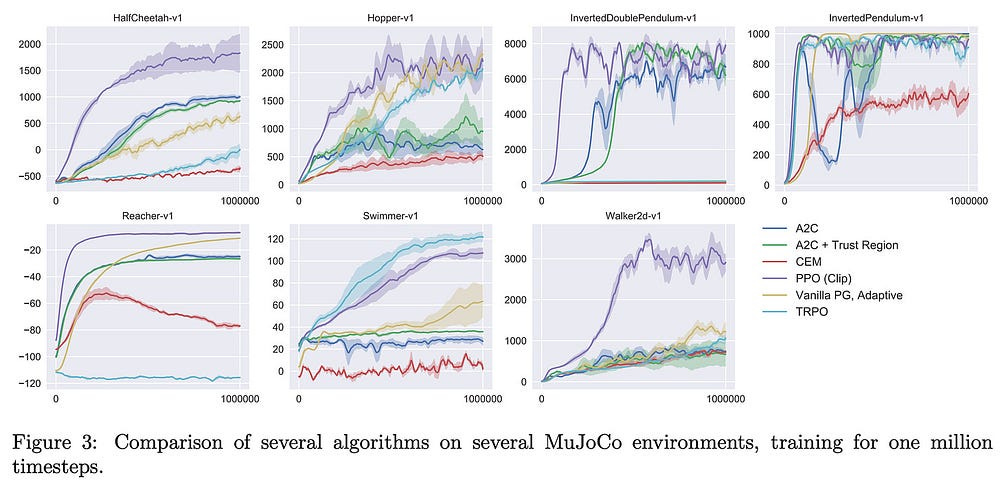
Proximal Policy Optimization (PPO): The policy and value networks are trained using PPO, a state-of-the-art RL algorithm that ensures stable and efficient learning. PPO fits the chip design problem perfectly because it handles challenging multi-objective rewards and enormous state spaces through conservative policy updates. By clipping the policy change magnitud, it prevents destructive updates when good placements are found — crucial since rewards only come after complete placement. PPO’s ability to collect experiences in parallel also enables efficient training, letting AlphaChip learn from multiple chip designs simultaneously, which is essential given the computational demands of placement evaluation.
Below is a good comparison of PPO against other techniques, from the brilliant
and his excellent coverage of PPO, “When PPO is compared to a variety of state-of-the-art RL algorithms on problems with continuous action spaces, we see that it tends to learn faster and outperforms prior techniques on nearly all tasks”-
Sequential Placement: The agent places macros one at a time, using the policy network to guide its decisions and the value network to evaluate the quality of its actions.
Reward Feedback: The agent receives a reward signal at the end of each placement episode, which is used to update the policy and value networks.
Both of these (+ the hierarchical placement) combine to create our high-performing chip designer. Given the very promising economics of this field, I think there is a lot of business value to be captured in this space, and I’m excited to see how it plays out.
Let me know what you think. Oh, and Happy New Year.
Thank you for reading and have a wonderful day.
Dev <3
If you liked this article and wish to share it, please refer to the following guidelines.
That is it for this piece. I appreciate your time. As always, if you’re interested in working with me or checking out my other work, my links will be at the end of this email/post. And if you found value in this write-up, I would appreciate you sharing it with more people. It is word-of-mouth referrals like yours that help me grow. You can share your testimonials over here.
Reach out to me
Use the links below to check out my other content, learn more about tutoring, reach out to me about projects, or just to say hi.
Small Snippets about Tech, AI and Machine Learning over here
AI Newsletter- https://artificialintelligencemadesimple.substack.com/
My grandma’s favorite Tech Newsletter- https://codinginterviewsmadesimple.substack.com/
My (imaginary) sister’s favorite MLOps Podcast (over here)-
Check out my other articles on Medium. : https://rb.gy/zn1aiu
My YouTube: https://rb.gy/88iwdd
Reach out to me on LinkedIn. Let’s connect: https://rb.gy/m5ok2y
My Instagram: https://rb.gy/gmvuy9
My Twitter: https://twitter.com/Machine01776819









Edge-GNN is so cool.
Edges aggregate information from nodes.
The nodes then aggregate neighbouring nodes along with edge embeddings.
Domain knowledge resulting in minor changes to a model goes a long way indeed!
Great content once again. Makes you get a glimpse into the chip wars that are about to heat up seriously